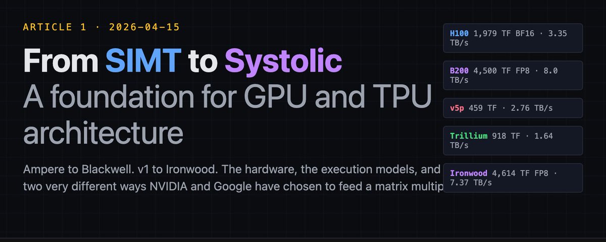
几周前,我离开了 Meta 的 Triton 编译器团队,加入了 Google 的 PyTorch/TPU 团队。这个转变差不多就是你能想到的样子。我在 GPU 栈里待了多年,为 Hopper 和 Blackwell 写过 lowerings,争论过 warpgroup intrinsics,写过成千上万个 benchmark 和几十个工具。现在,我盯着脉动阵列,心里想的是,为什么文档里没人这么叫它们。
这是我写过最长的一篇文章。它长,是有意为之。我想写一篇能同时服务四类读者的文章。如果你从没认真想过 ML 硬件,第一部分是给你的。如果你懂分布式训练,但不熟悉加速器架构,Part 2A 和 2B 会带你穿过两边,而且不假设你已经懂另一边。如果你已经熟悉 CUDA,只想看 TPU 这条线,你会先得到一次不错的复习,然后进入 TPU 的重点。如果你写 kernel,或者做编译器,整篇都会有东西可拿;而 Article 2 会展开编程模型上的论证。我真的没法把所有好东西塞进 X 的文章字数限制里。
到这个系列结束时,我会试着说服你,哪怕是在 GPU 本该完全占据优势的领域,也就是自定义 kernel 编写,TPU 也是更好的平台。这是一个很强的判断,我也不指望靠感觉赢。下面我会先把基础铺好,等到第二篇文章结束时,你会被说服。
开始前最后说一句。我两套栈都用。工作需要时,我仍然会写 Triton,也会写其他 DSL。在 TPU 上构建新算子时,我仍然需要 GPU 来做对比。这不是宗教战争。这是一个判断:哪一组架构选择,会在事实层面产生复利。
加速器为什么存在
CPU 的形状来自一个判断:大多数程序有大量分支,内存访问不可预测,并且奖励单线程低延迟。所以,一个现代 CPU 核心会把大部分硅面积花在分支预测器、乱序调度器、投机执行机制,以及那些很努力地让不可预测代码看起来很快的缓存上。相比之下,算术单元很小。一个 Xeon 核心可以做出很可观的 FLOPs,但晶体管并不是主要花在 FLOPs 上的。
然后,深度学习出现了。现代 ML 工作负载来自另一种判断。主导操作是收缩。全连接层里的 matmul,attention 里的 matmul,到处都是 batched matmul。这些操作可预测,循环密集,几乎不花时间在分支上。运行前,你就知道循环边界。运行前,你就知道内存访问模式。运行前,你就知道算术强度。
如果盯着这件事看得够久,你会发现,理想硬件的形状几乎和 CPU 相反。你希望大部分硅面积都在做乘法和累加。你不需要分支预测器,因为没有分支。你不需要投机执行,因为没有不确定性。你也基本不需要巨大的缓存,因为访问模式是密集数组的分块,你可以手动暂存它。
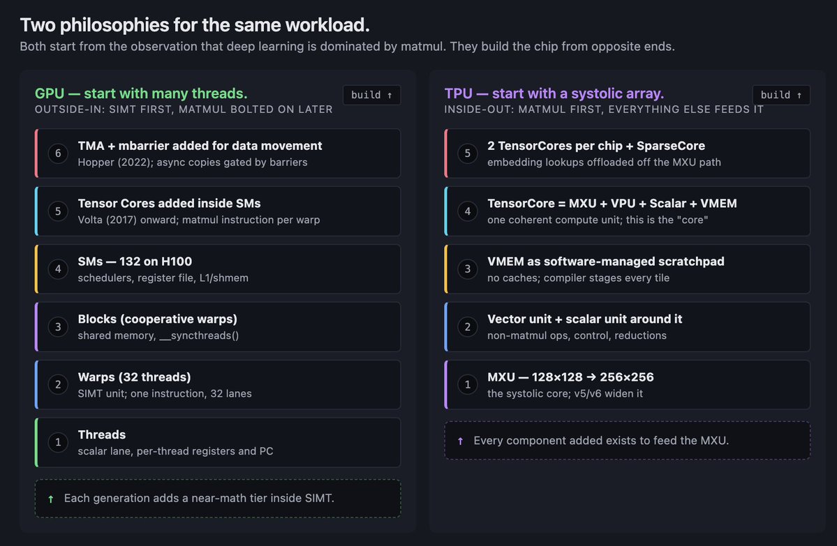
加速器来自认真对待这个观察。NVIDIA 走了一条路。Google 走了另一条路。两条路都从同一个根本事实出发:工作负载由少数几类收缩操作主导,所以硬件也应该由矩阵单元主导。芯片上的其他东西,都是为了让这些单元不断粮。
在 GPU 上,我们原本甚至不是在解决这些问题。Shader 和其他图形计算机制,碰巧成了未来的好地基。对 GPU 来说,答案是从一个已经擅长图形的并行线程底座出发,在每个 streaming multiprocessor 里加入叫 Tensor Core 的矩阵引擎,然后让成千上万个线程掩盖把数据送到这些单元时产生的延迟。对 TPU 来说,答案是直接丢掉大部分调度机制,把一个巨大的脉动阵列放在芯片中央,再让编译器围绕它编排数据移动,让阵列永远不饿着。
同一个观察,两种哲学。本文剩下的部分,就是讲这些哲学跨越几代之后会发生什么。
这里有一条底层轴线,值得现在就点出来。CPU 优化延迟:让一个线程快。GPU 通过过量提交优化吞吐:准备足够多的线程,让机器总有活干。TPU 通过确定性优化吞吐:提前调度每个操作,并通过构造方式让流水线保持满载。延迟对吞吐;在吞吐内部,是过量提交对确定性。这就是每个加速器架构师都不得不选择的三个位置。
内存墙
下面这个事实,会塑造本文中所有其他选择。算术相对便宜。移动数据很贵。差距不小,而且每年都在变大。
在现代加速器上,一次矩阵乘的能耗是个位数皮焦。从片上 SRAM 读取一次,能耗大约高一个数量级。从 HBM 读取一次,大约是乘法本身能耗的 100 倍。通过主机 CPU 的内存总线从 DRAM 读取,又比 HBM 高一个数量级。这里只是在说能耗。时间成本也呈现同样的形状。matmul 是纳秒级。HBM 访问是数百纳秒。PCIe 或 NVLink 往返是微秒级。跨数据中心跳转是毫秒级。
本文里每一个架构决策,都是对这个差距的回应。这些文章里你会遇到一袋缩写词,每一个都是在用不同方式说同一句话:缩短数据所在位置和数学发生位置之间的距离。现在不用急着记术语。只要知道,它们全都在回答同一个问题。
你可以把 ML 加速器的整个演化,看成一场缩短数据和数学距离的战役。芯片变大。内存变近。网络变平。编译器做更多事。每一代,FLOPs 和移动字节数的比例都会上升,这意味着软件必须更努力,才能让机器吃饱。
不见过几次很难意识到的一点是:这不是靠更多带宽就能解决的问题。HBM 每一代都在变快。它仍然不够快。Ironwood 每芯片 7.37 TB/s 的 HBM3e 听起来已经离谱,直到你注意到这颗芯片能做超过 4.6 PFLOPS 的 FP8,于是比例还在继续爬升。带宽追不上。比例会变得更糟。你无法跑赢内存墙,只能绕着它跳舞。
这就是为什么任何人教 kernel 编写时,第一件事都是 tiling。把数据分块。移动一次 tile。尽可能在再次移动它之前,对它做更多数学。加速器上的每个优化故事,最后都会塌缩成一个数据暂存故事。硬件把策略说得很明白。编译器、库、手写 kernel,最后都会编码同一条规则的某个版本:让数据尽可能长时间待在离算术单元近的地方,只有绝对必要时才把它溢出。
记住这条规则。后面你会再次看到它。TMA 是这条规则。producer-consumer warpgroups 是这条规则。emit_pipeline 是这条规则。torus topology 也是这条规则。本文里的一切都是这个主题的变体,因为内存墙就是那个不会消失的东西。
真正重要的算术
这一节里,只靠一个概念你就能走很远:算术强度就是每移动一个字节,你做多少次浮点操作。就这样。FLOPs per byte。
两个 [N, N] 矩阵相乘,大约做 2N^3 次 FLOPs,移动大约 3N^2 字节,忽略复用的话就是两个输入和一个输出。算术强度随 N 增长。tile 越大,每移动一个字节做的数学越多,越好。一次逐点加法的算术强度基本为零。你移动两个字节,做一次 FLOP,再写一个字节。无论如何都是 bandwidth-bound。
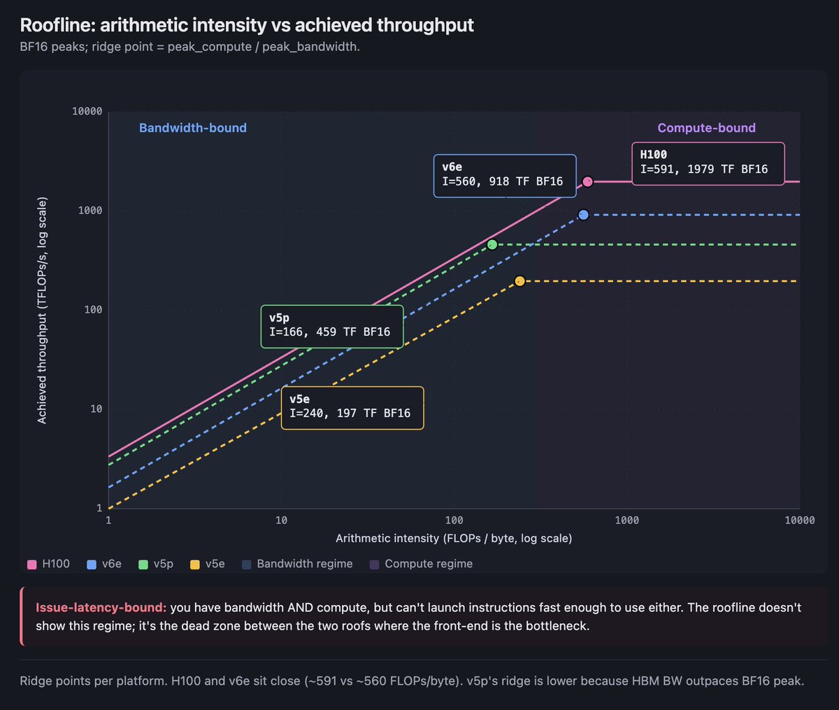
roofline model 把这件事拼在一起。横轴画算术强度,纵轴画实际达到的每秒 FLOPs。你会得到两条屋顶线。平的屋顶是芯片的峰值计算能力。斜的屋顶是带宽上限:强度越高,每移动一个字节能做的 FLOPs 越多,就越接近峰值。两条屋顶相交的地方叫 ridge point。低于 ridge 的操作是 bandwidth-bound,除了让操作更密集之外,你什么也做不了。高于 ridge 的操作是 compute-bound,问题就不是总线,而是怎么让矩阵单元不断粮。
还有第三种状态,没人画在图上:issue-latency-bound。你有带宽,也有计算能力,但无法足够快地发射指令来用满两者。GPU occupancy discipline 就来自这里,TPU 编译器的 instruction-packing 工作也在这里产生价值。
来自 HBM 的具体 ridge point,因为具体数字能让模型更牢:
-
H100 SXM5:Tensor-Core BF16 峰值 1,979 TFLOPS,HBM3 带宽 3.35 TB/s,得到的 ridge point 大约是每字节 591 FLOPs。
-
TPU v5e:用同样方式推导,大约是每字节 240 FLOPs。
-
TPU v5p:大约是每字节 166 FLOPs。pod 比 v5e 扩得更大,但单芯片 ridge point 反而更低,因为 v5p 的 HBM 带宽增长超过了 BF16 峰值。
-
TPU v6e(Trillium):大约是每字节 560 FLOPs。这是一次大跳。
带着两个具体数字往后看。v5e 在 BF16 下,每个 replica 大约需要 240 个 token 的 batch,才能站到来自 HBM 的 ridge point 之上。如果使用 int8 activations 和 bf16 weights,这个数字会降到大约 120。在 H100 上,由于 ridge point 会和更深的缓存、更灵活的调度互动,你可以用更小的有效 batch 勉强过关。TPU 要你认真思考 batch size。GPU 允许你更久地忽略它,但也只是到某个点为止。
如果这一整节只记一件事,就记这个:ridge point 会告诉你,你现在跑的是内存问题还是计算问题,而答案会改变哪些优化真的有用。
精度和 dtype
对抗内存墙的另一个杠杆是精度。每一个不移动的 bit,都是你不用付出的成本。所以,加速器在过去近十年里,一直沿着 bit-width 下探。
在走过这些名字之前,先带着一个心智模型。尺度很小时,现代技巧是 microscaling:你用小格式存数,比如四位或八位;再为一小组值单独存一个 scaling factor;硬件在做数学时把 scale 乘回去。存储和带宽主要由小格式决定。准确性来自 scale。你下面看到的每一种 sub-byte format,都是这个技巧的某种变体。
训练 dtype。 FP32 是旧基线。密集、准确、昂贵。TF32 是 NVIDIA 的发明:在 FP32 范围里使用 19 位 mantissa,通过 Tensor Cores 运行,在 Ampere 上作为 FP32 的直接替代。BF16 是今天占主导地位的训练 dtype。它像 FP32 一样有 8 个 exponent bits,7 个 mantissa bits,所以保留范围,牺牲精度。从 PaLM 到 Llama,再到当前前沿模型,所有严肃训练栈都用 BF16 加 FP32 accumulation 训练。FP16 早于 BF16,现在仍然存在,主要用于向后兼容和推理。它的 exponent 太小,不做 loss-scaling 之类的体操就很难训练,这也是 BF16 在训练侧取代它的原因。
推理和小占用 dtype。 Hopper 引入了两种 FP8:E4M3 用于 forward pass 和推理,E5M2 用于 backward pass 和 gradient storage。Hopper 上的 Transformer Engine 会跨 step 跟踪 activation statistics,并为每个 tensor 应用 scaling factor,避免 FP8 在数值上崩掉。Blackwell 用 NVFP4(四位、两级 scaling)和 MXFP8(八位 microscaling)扩展了这条路。INT8 是 TPU 上长期存在的推理 dtype;Trillium 每芯片达到 1,836 TOPS 的 INT8,我们会在 §2B.3 看到 Trillium。Ironwood 把原生计算迁到了 FP8。TPU 谱系的其他部分在 Ironwood 之前对精度一直比较保守,因为 Google 的判断是,仔细编译可以从 BF16 中榨出大部分吞吐,不必依赖 sub-byte formats。
有一条历史经验值得带着。每一代向下跳精度的产品,客户采用率也会随之跳升,因为人们真正撞上的约束是内存带宽,而把带宽需求砍半,往往比把峰值 FLOPs 翻倍更有用。精度故事和内存墙故事,其实是同一个故事。
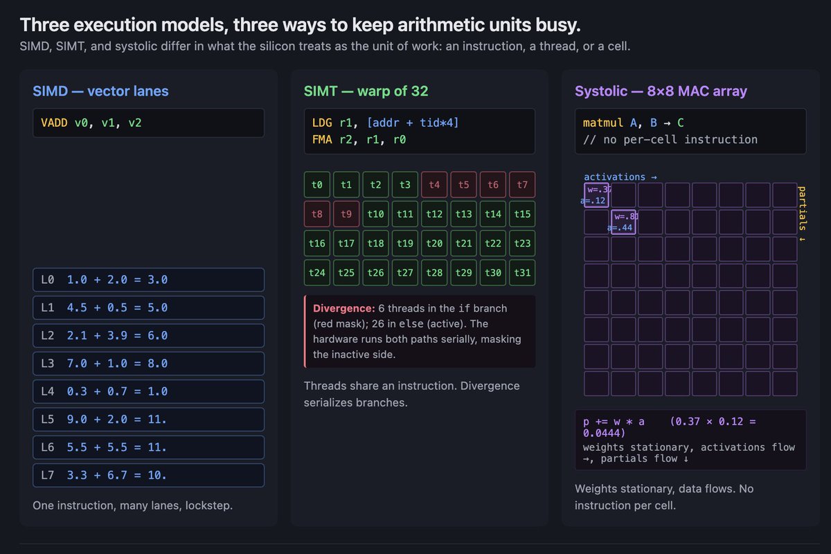
三种执行模型
加速器最终基本都在实现三种执行模型之一。理解这三种模型,是你读完本文剩下部分而不迷路的关键。
SIMD 是最古老的。Single Instruction, Multiple Data。你有一定数量的 lane,发射一条指令,每个 lane 在自己的数据上执行它。CPU SIMD(AVX、SSE、NEON)就是这样。早期 GPU 上的 vector units 也是这样。SIMD 很精简,因为所有 lane 共享一个 instruction pointer,但它很僵硬。如果 lane 需要做不同的事,你要么 mask 它们,要么 stall。
SIMT 是 NVIDIA 的发明,也是现代 GPU 的定义性模式。Single Instruction, Multiple Threads。想象一个指挥家带领 32 人乐团:一次下拍让所有乐手同时动作,但每个人读自己的谱。这就是 SIMT。你写的代码看起来像是在一个线程上运行。硬件把线程组织成 32 个一组的 warp,并在底层让 warp lockstep 运行,所以在抽象之下,它实际上像 SIMD。但编程模型看起来像线程:每个线程有自己的 program counter、自己的 registers、自己的控制流。当一个 warp 里的线程需要做不同的事,就会出现 warp divergence。硬件会串行化分支,先运行一条路径,同时 mask 另一边的 lane,然后再运行另一条路径。它能工作,但会消耗吞吐。
SIMT 是 GPU 让人觉得高效好用的原因。你写的 kernel 看起来像并行循环。硬件处理 lockstep execution、memory coalescing,以及通过 warp-level overcommit 隐藏延迟。大多数时候,你不用考虑物理 lane。当你不得不考虑时,通常是撞上了这个抽象的锋利边缘:warp divergence、uncoalesced memory accesses、register pressure、shared memory bank conflicts。这些锋利边缘,就是 GPU kernel 优化像一门手艺的全部原因。
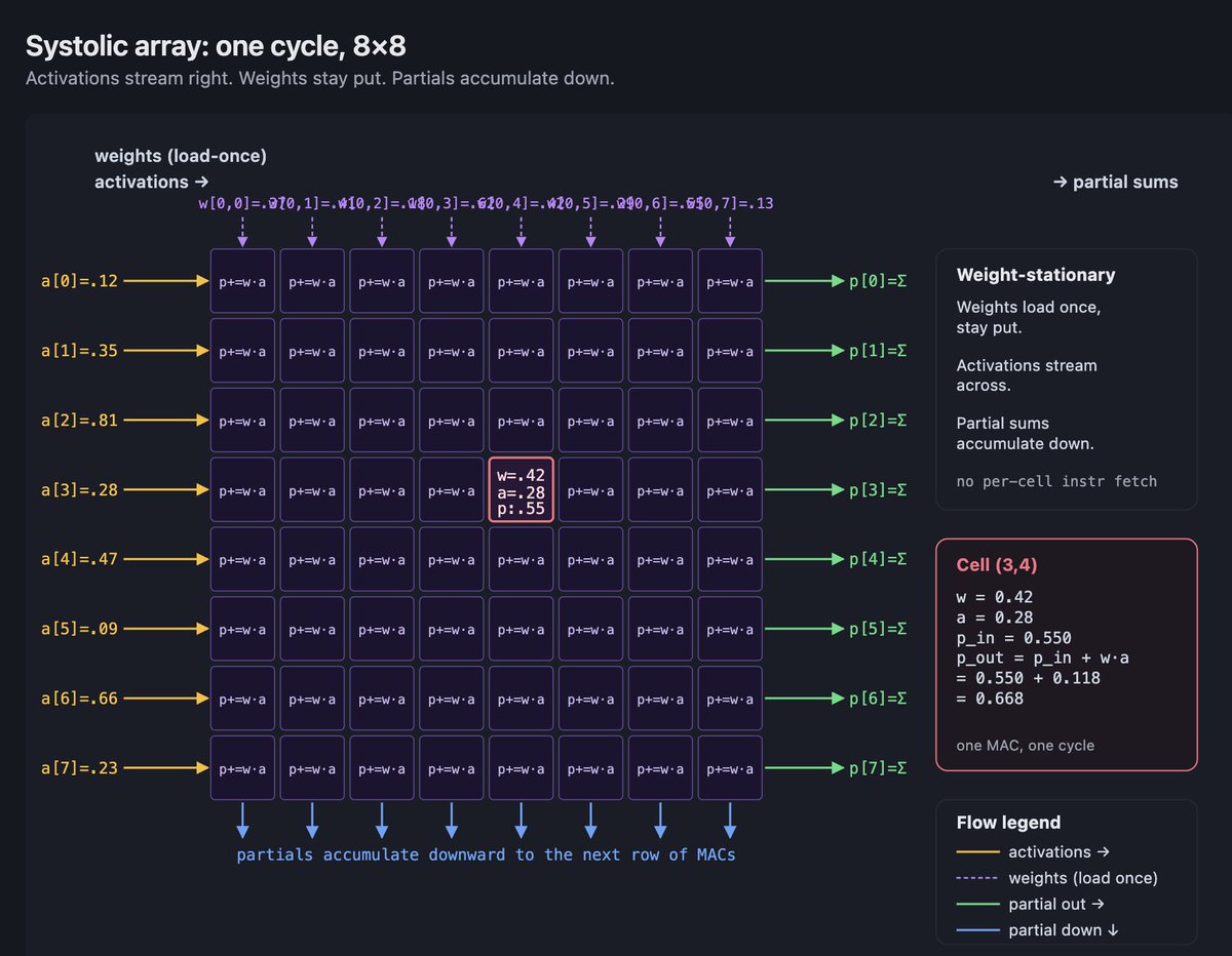
Systolic 是 TPU 漂亮的答案。脉动阵列是一个二维 multiply-accumulate 单元网格,它们互相连线,让数据像水穿过网格一样流动。每个 cycle,每个 MAC 单元从邻居那里拿一个值,用一个 stationary weight 做 multiply-add,或者根据 dataflow 使用 streaming weight,然后把结果交给下一个邻居。每个单元不需要 instruction fetch。不需要控制逻辑。只有数据穿过算术网格时的节奏。
收益是密度。如果每个 MAC 单元不需要取自己的指令,也不需要管理自己的 registers,你就能在每平方毫米里塞进更多 MAC 单元。一个 256×256 的脉动阵列有 65,536 个 MAC 按节奏工作。代价是僵硬:阵列以固定形状工作,任何不是 matmul 形状的操作,都必须发生在阵列旁边的 vector 或 scalar units 里。这也是 TPU 为什么如此在意 tile shapes。pad 太多会浪费网格。填不满会浪费 cycle。
稍微眯着眼看,你能在同一张图里看到三种模型。SIMD 是许多 lane 中的一条指令,lockstep。SIMT 是许多 lane 的许多 lane,上面盖着一个线程幻觉。Systolic 是固定功能单元的网格,数据按编排流过。SIMD 在规则代码上赢吞吐。SIMT 在规则代码上保留良好吞吐,同时赢生产力。Systolic 在矩阵形状代码上赢密度。每种加速器架构都是某种混合。
两种哲学
接下来所有内容,都可以通过一个分裂来读。这个分裂出现在 NVIDIA 和 Google 做过的每个架构选择里。
NVIDIA 的哲学,从程序员往里读:从许多并行线程开始。围绕它们构建内存层级。在每个 streaming multiprocessor 里加入矩阵引擎,让线程可以集体发射矩阵指令。随着时间增加功能,让线程更紧密地协作,像 warpgroups、thread block clusters、distributed shared memory。线程先在那里。其他一切都围绕它们适配。
Google 的哲学,从相反方向读:从矩阵 dataflow 开始。把 MXU 放在芯片中央。加入 vector unit 处理那些不适合 MXU 的东西。加入 scalar unit 做控制。加入 VMEM,让编译器能把数据暂存成 MXU 能消费的形状。加入 ICI,让芯片可以不经过 HBM 就交换 tile。脉动阵列先在那里。其他一切都围绕它适配。
这些不只是组织差异。它们会复利。一旦 NVIDIA 承诺 SIMT,之后每个设计决策都必须让线程更有生产力:shared memory、Tensor Cores、warp-level intrinsics、TMA、mbarrier、cluster APIs。一旦 Google 承诺脉动阵列,每个决策都必须喂饱它:确定性的 VMEM staging、compiler-scheduled DMAs、torus fabrics、sparse-core offload,用来处理 MXU 吸收不了的操作。
随着抽象成熟,GPU 会变得更容易编程。随着编译器成熟,TPU 会变得更有吞吐密度。GPU 的下限,也就是写显而易见代码能拿到的东西很高,因为 runtime 帮你做了很多事。TPU 的上限,也就是写 compiler-aware code 能拿到的东西很高,因为没有东西浪费在运行时动态性上。两种哲学没有哪种严格更好。它们产生的是不同形状的好。
当你读到 Hopper 上的 TMA,请注意这是 GPU 侧承认 compiler-scheduled data movement 是正确方向,并试图在 SIMT 抽象里触达它。当你读到 Ironwood 的 FP8 和 OCS fabric,请注意这是 TPU 侧从相反方向到达与 Blackwell 相同的尺度:让 systolic core 足够快,让 fabric 足够大。两种哲学,同一个目的地,非常不同的形状。
从这里开始的提醒
这篇文章有意写得很长。需要的话,分几次读。它本来就是按这种方式写的。
Part 2A:NVIDIA 这条线
GPU 基础入门
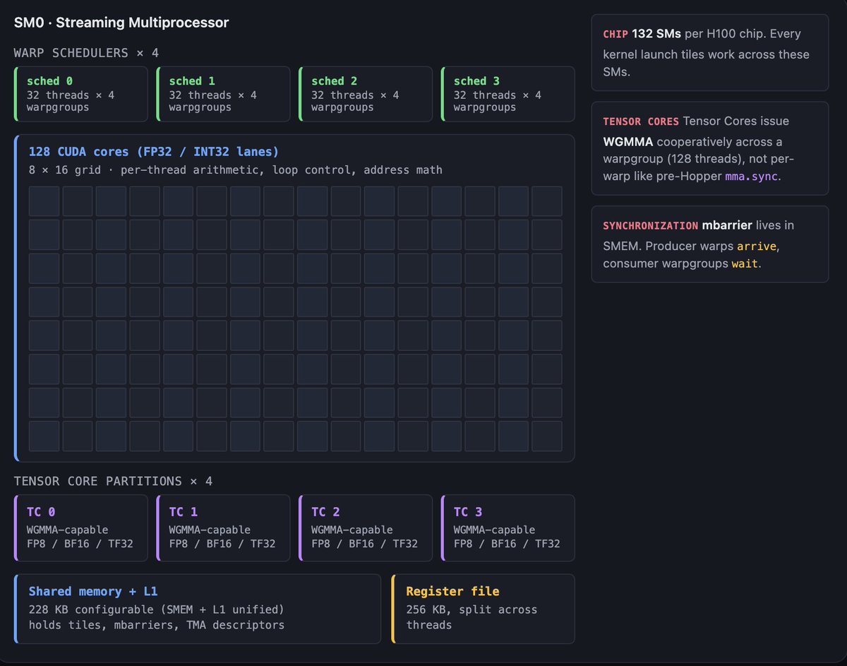
在讲 Ampere、Hopper 和 Blackwell 之前,你需要在脑子里带着一张图。我用文字描述它。
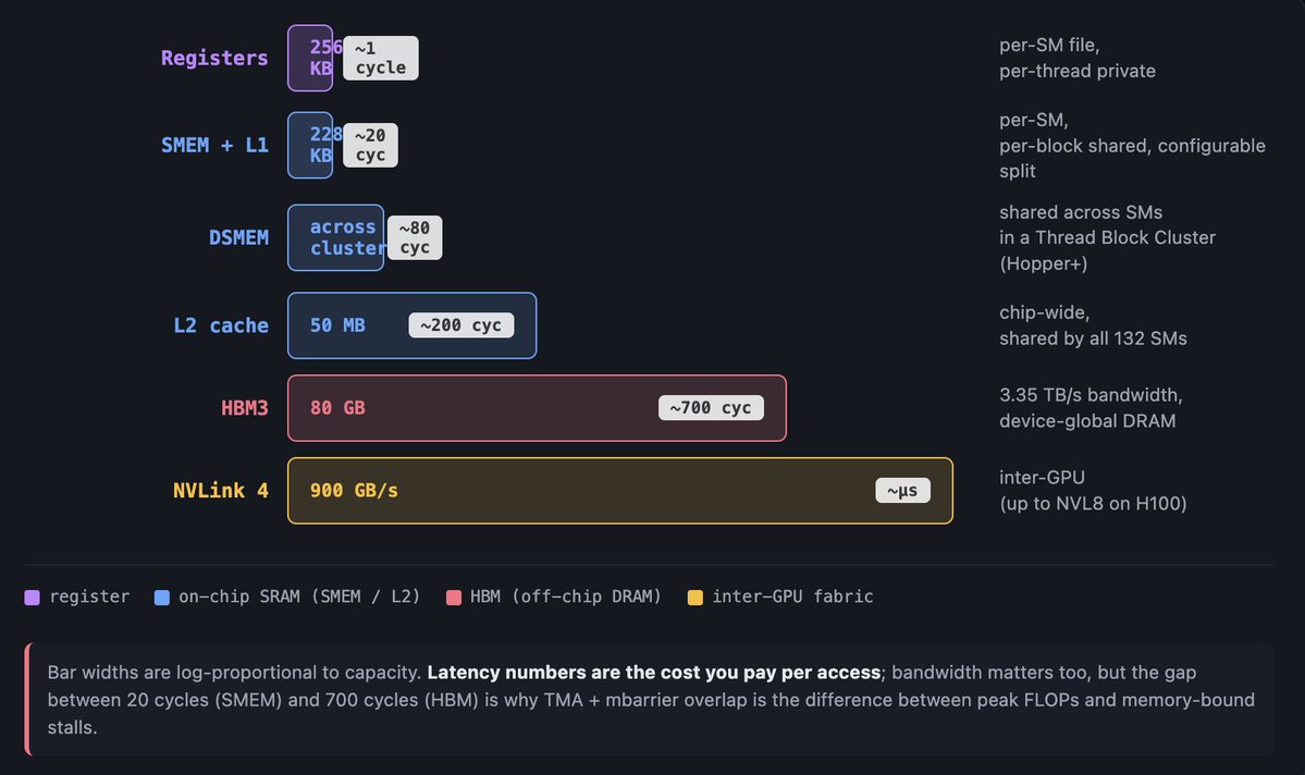
现代 NVIDIA GPU 是一个 streaming multiprocessors(SM)网格。H100 有 132 个。B200 更多。每个 SM 是执行单元。当你 launch 一个 kernel,GPU scheduler 会把 thread blocks 分配给 SM。block 会在拿到它的 SM 上运行到完成。如果 registers 和 shared memory 允许,一个 SM 可以同时容纳多个 block。
在单个 SM 里面,有用于 scalar 和 vector FP arithmetic 的 CUDA cores,有少量用于 transcendentals 的 special-function units,还有 Tensor Cores,也就是矩阵引擎。Tensor Cores 是 SM 里唯一能以接近峰值速率做密集矩阵数学的部分。如果你没有发射 Tensor Core instructions,你就跑在慢路径上。
线程被组织成 32 个一组的 warps。Warps 是 SIMT 执行单位:32 个线程,一条指令,大多数时候一个 program counter。多个 warp 组成一个 thread block,这是程序员调度的单位。Thread blocks 共享一块 shared memory(SMEM),它是 physically located in the SM 的片上 SRAM。一个 block 内的线程可以便宜地同步。跨 block 的线程不行。
SM 外面的内存层级是这样:L1 cache 位于每个 SM 中,在现代 GPU 上和 SMEM 物理统一,你在二者之间分配预算。L2 cache 由芯片上所有 SM 共享。HBM 是片外主内存。越往外,每一层越慢,也越大。Registers 最近也最小。HBM 最远也最大。kernel 编写的游戏,就是把数据往内存层级上方移动,并在它回落之前做尽可能多的数学。
如果你看到这些词而疑惑,这里先给三个词汇:warp divergence,一个 warp 里的线程走不同分支时会顺序运行,所以吞吐下降;coalescing,来自一个 warp 的相邻地址 load 会被合并成一次 transaction;occupancy,一个 SM 保持多少 warp in flight 来隐藏 stall。如果你不写 kernel,可以放心略过这些。Tensor Cores 相比 CUDA cores 不那么在意 occupancy,因为它们有专用路径和自己的调度。
这些足够读完 Part 2A 的剩余部分了。我们讲的每一代,都会往这张图里加东西。Ampere 加入 TF32 和 async copies。Hopper 加入 warpgroups、TMA 和 mbarrier。Blackwell 加入 TMEM,并把 Tensor Cores 从 warp scheduler 中解耦。底层形状保持不变。
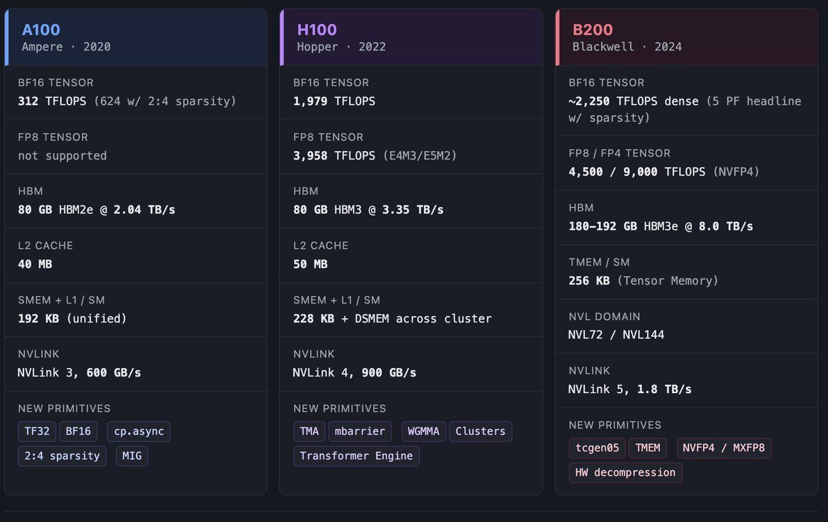
Ampere / A100
A100 是 NVIDIA 停止假装这是一颗图形芯片的一代。每一份 Ampere 技术说明读起来都像数据中心白皮书,因为它本来就是。它也是 大多数 GPU 专用 DSL 所基于的芯片。理解 Ampere,至今仍是理解几乎每一种 DSL 的关键。
我认为,对 kernel 作者来说,最有后果的新增能力是 cp.async。它可以把数据从 global memory 直接移动到 shared memory,而不经过 register spill。Ampere 上的版本是半异步的,意思是你发出 copy,去做别的工作,最终在 completion 上 fence。Hopper 上现代的 TMA+mbarrier 模式,就是这个想法的完全异步版本。Ampere 上的 cp.async 是第一次尝到这个味道。
A100 有 80 GB 的 HBM2e,带宽 2,039 GB/s;Tensor Cores 提供 312 dense BF16 TFLOPS,使用 2:4 sparsity 时是 624;还有 MIG(Multi-Instance GPU)分区,给那些想把芯片切成更小加速器、用于多租户工作负载的云服务商。MIG 听起来枯燥,但它是重要背景:到了 A100,NVIDIA 设计的不只是整芯片工作负载,也包括被租出去的一片片芯片。
重新算 roofline:A100 来自 HBM 的 ridge point 是 312 × 1000 / 2,039 ≈ 每字节 153 FLOPs。这个数高于 BERT 和 ResNet 规模 matmul 所在的位置,低于密集 transformer training 所在的位置。A100 不需要像后来的几代那样担心 ridge point。
A100 定义了现代 ML training 的 下限。在它之后的一切,都至少假设有这个硬件水平。如果你读 2021 到 2023 年的论文,里面说“我们在 8 个 GPU 上训练”,你大概率可以在脑中把它替换成“8 个 A100”,而且通常不会错。
2A.2 Hopper / H100
Hopper 是本文的锚点世代,因为 Hopper 是数据移动不再只是副作用,而是成为程序本身的一代。
在缩写词出现前,先用白话说。Hopper 之前,GPU 线程是让 copy 发生的东西:你写循环,线程执行每一次 load。Hopper 之后,你给硬件一段 copy 的简短描述:“从 HBM 取这个 tile,用这个 layout 放到 shared memory”,然后硬件在你的线程去做其他工作时完成剩下的事。本节剩余部分,就是让这个变化成真的机制,也是你以后读到的每个优化 H100 kernel 都长成那样的原因。
我想逐步建立这个判断。A100 已经有 cp.async,已经有 Tensor Cores,已经有 BF16。H100 的新功能不是孤立的 bullet points。它们共同改变了 kernel 是什么。
Thread Block Clusters 是执行层级中的新一级。旧图景里,threads 组成 warps,warps 组成 blocks,blocks 组成 grid,而 blocks 之间不能通信。在 Hopper 上,相邻 block 可以被组成一个 cluster,通常是 4 或 8 个 blocks,cluster 会被调度到一组连续的 SM 上。cluster 内的 block 可以访问彼此的 shared memory。这叫 Distributed Shared Memory(DSMEM)。底层看,它是 SMEM 加上 cluster 内 SM 之间的物理互连。DSMEM 不像本地 SMEM 那么快,但比出去到 L2 或 HBM 快得多。
DSMEM 重要,是因为它允许你把操作跨多个 SM 分块,而不必付通过 L2 共享数据的往返成本。过去一个 SM per head 的 flash-attention 风格 kernel,现在可以一个 cluster per head,并让 per-head 数据在多个 SM 之间协作保持。
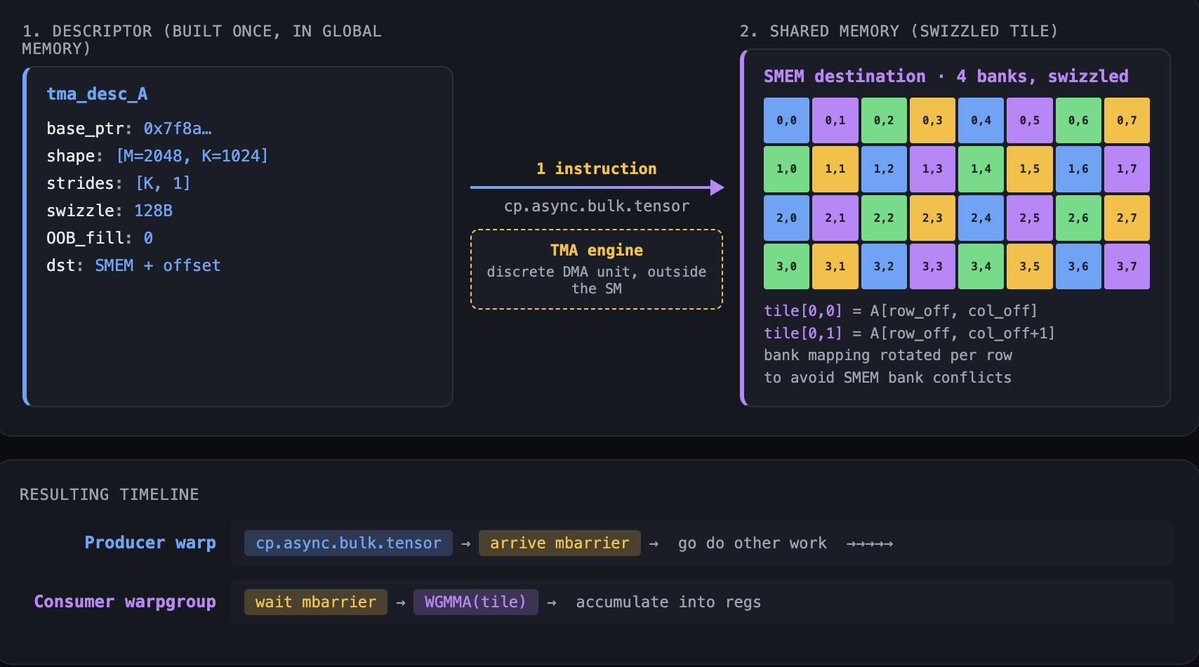
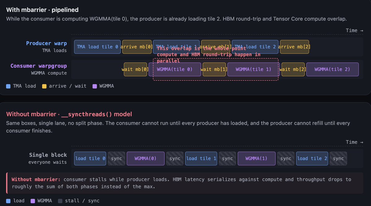
Tensor Memory Accelerator(TMA) 是重新排列一切的功能。TMA 是 descriptor-driven async copy engine。你构造一个 descriptor 描述 source tensor,包含 base pointer、shape、strides、swizzle pattern、out-of-bounds fill value;再构造一个 descriptor 描述 shared memory 中的 destination tensor;发出一条指令,DMA engine 就会移动 tile。写循环的是编译器,不是线程。发出 TMA 的 warp 可以在 copy 运行时去做其他工作。
TMA 有三件重要的事不会出现在规格表上。第一,TMA 在硬件中处理 bounds checking 和 padding。如果你的 tile 超过 tensor 边界,TMA 会用指定值填充,而不是 trap。这会从 kernel code 中消灭一整类 tail-case branches。第二,TMA 可以在 copy 过程中应用 swizzle patterns,让数据以一种避免 Tensor Cores 读取时 bank conflicts 的 layout 落进 shared memory。第三,TMA 是 cluster 上 multicast 的底座。一次 TMA 可以把同一个 tile 同时落到 cluster 内多个 SM 的 SMEM 中,替代原本需要的 N 次独立 loads。
Warpgroup MMA(WGMMA) 是新的 Tensor Core instruction family。一个 warpgroup 是四个 warps,也就是 128 个线程。不同于以前运行在单个 warp 上的 mma instructions,WGMMA 是 warpgroup-cooperative:指令由四个 warp 一起发出,硬件调度一个更大的矩阵操作,把 issue cost 摊到更多线程和更多数据上。WGMMA 可以直接从 shared memory 取 operands(RS-stage),不用先搬到 registers,这是巨大的带宽收益。
mbarrier 是把这条流水线绑在一起的同步原语。GPU 上经典的 shared-memory sync 是 __syncthreads(),像一道悬崖:block 里的每个线程都要等到所有其他线程到达。简单模式下这很好,但对 overlap 来说很糟。mbarrier 是 split-phase barrier:你可以让一个 warp arrive,另一个 warp wait。这让 producer-consumer pattern 成立。一个 warp 发出 TMA load,在 mbarrier 上 arrive,然后继续。另一个 warp 在 mbarrier 上 wait,用 WGMMA 消费数据,再在另一个 mbarrier 上 arrive,表示这个 tile 空出来了,然后继续。除非流水线从根上卡住,否则 warps 不会 stall。
Hopper 上的 FP8 是 E4M3 和 E5M2,配合 Transformer Engine 通过 delayed-scaling protocol 跨 step 跟踪 per-tensor scales。Delayed scaling 的意思是,你跟踪前几次 iteration 的 amax,并用它来 scale 当前 iteration,这样不用为在线计算 scale 付同步成本。只要做得仔细,FP8 training 在相关任务上的 accuracy drop 接近于零。带宽节省则很有意义。
内存层级方面:HBM3 3.35 TB/s,50 MB L2,比 A100 的 40 MB 提升;cluster 间有 DSMEM;每个 SM 的可配置 SMEM+L1 预算也更大。NVLink 4 每 GPU 900 GB/s,聚合在 NVL8 和 NVL64 server topologies 中。数字重要,但真正重要的是,层级中的每一层都变快了,而且新增了一个 near-math level,也就是 DSMEM。
现在功能都摆上桌了,可以说那个判断了。Hopper 之前,kernel 是“做算术,然后围绕它协调一点内存移动”。Hopper 之后,kernel 是“调度内存移动,而算术发生在移动留下的空隙里”。一个调好的 H100 matmul 主循环,是 producer warp 把 TMA loads 发进 circular SMEM buffers,consumer warpgroups 通过 WGMMA 从这些 buffers 中拉数据,mbarrier chains 把整条流水线 gate 起来。你可以用 CUDA 手写这个循环。你可以从 CUTLASS 得到自动生成版本。也可以让 Triton 替你写。
Triton 会这样处理它:
这就是整个 kernel。三十行。读起来像教科书里的 tiled matmul。现在看看 Triton 编译器在 Hopper 上实际发射了什么。如果你不是 kernel 作者,可以略过下一段:重点只是,编译器把三十行看起来无害的代码,变成了我们刚刚搭起来的完整 Hopper pipeline。
a = tl.load(a_ptrs) 和 b = tl.load(b_ptrs) 这两处 tl.load 会变成 TMA descriptor constructions 和 cp.async.bulk.tensor instructions。编译器选择一个匹配 WGMMA operand layout 的 swizzle pattern。遍历 K 的 for-loop 会变成一个 software-pipelined loop,里面有 multi-buffered SMEM staging、producer-consumer warpgroup split,以及一串 mbarrier arrives/waits gate 每个 stage。tl.dot 会变成由 consumer warpgroups 协作发出的 WGMMA instruction,尽可能直接从 SMEM 读取。最后的 tl.store 会变成 grid-striding TMA store。
这些都不会出现在 kernel source 里。Triton 的完整主张是,tile 是抽象单位,编译器根据你的目标 GPU 判断该怎么做。在 A100 上,同一个 kernel 会发射 cp.async 而不是 TMA,mma.sync 而不是 WGMMA,并使用经典的 __syncthreads() 模式,而不是 mbarrier。同一份 source,不同的 codegen。这就是 Triton 在做它该做的事。
这个 snippet 会在 Article 2 再次出现。Pallas 对比不是在比哪个 kernel 更短。它讨论的是编译器边界上发生了什么,以及每套栈怎样理解抽象。现在,只要注意这三十行隐藏了多少 Hopper-specific hardware。
Blackwell / B200 和 GB200
如果你刚接触这些,最短总结是:Blackwell 把 Hopper 的核心想法,也就是 async data movement、cooperative Tensor Cores、close-to-math memory,做得更大,并推得更远。两个新节拍是:NVLink domain 就是 机器,72 个 GPU 在一个 fabric 中,而不是 8 个;warp scheduler 不再控制 Tensor Cores,它们有了自己的 issue path。
先说明限制:Blackwell 的公开微架构披露比 Hopper 少,所以我会区分哪些是明确的,哪些是指示性的。
明确的是:B200 是一个 dual-die 芯片,有 10 TB/s 的 die-to-die interconnect(NV-HBI),并对程序员呈现为一个逻辑加速器。你不需要直接管理两个 die;CUDA 把这对 die 当作一个 device。每个 die 有自己的 SM 和自己的 HBM stacks。
明确的是:每 GPU 汇总 8 TB/s 的 HBM3e,容量 192 GB,指高配 B200。这比 H100 的带宽超过 2 倍,容量也超过 2 倍。由于 compute 增长更快,compute-to-bandwidth ratio 仍然收紧,但原始内存预算变得友好多了。
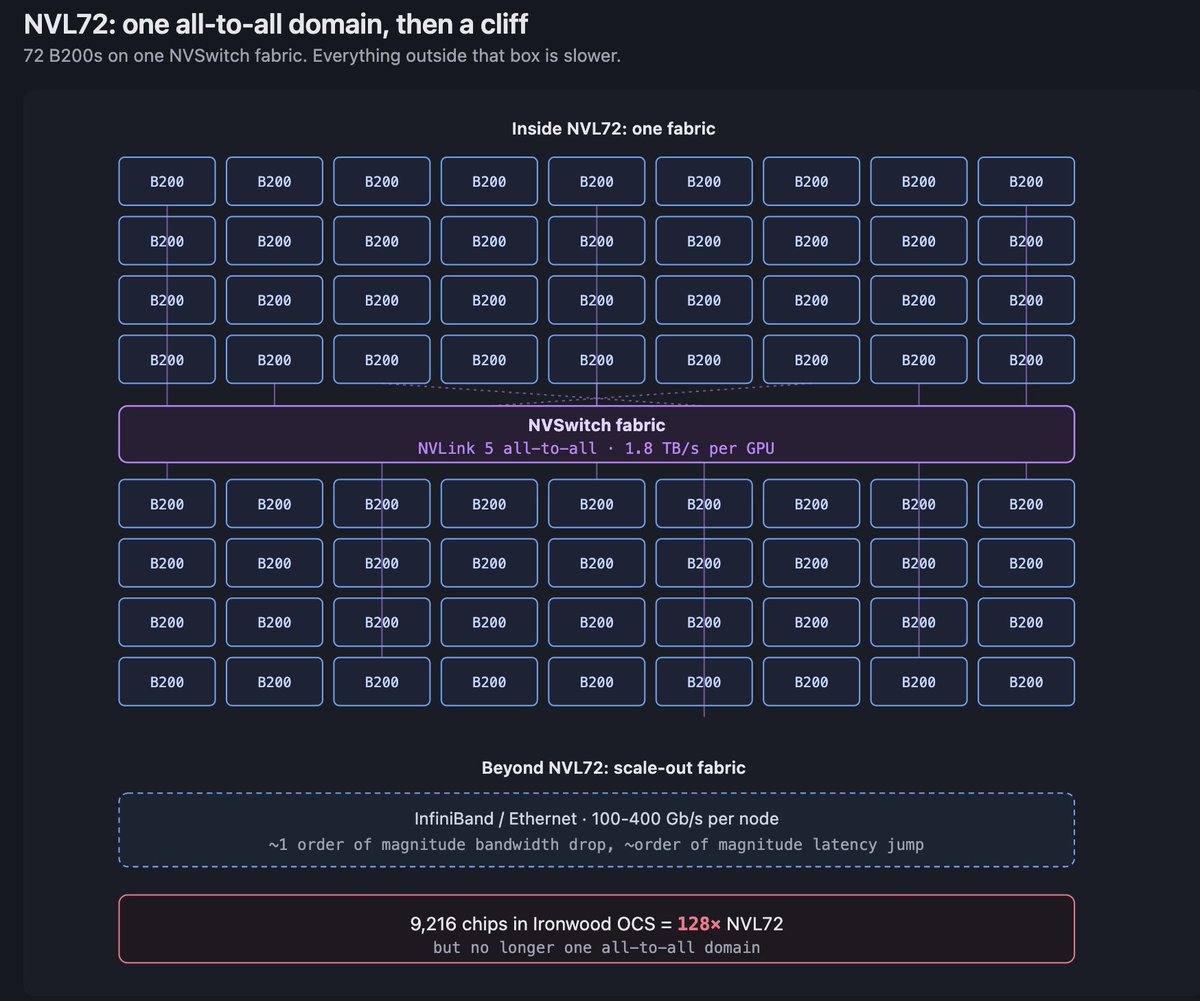
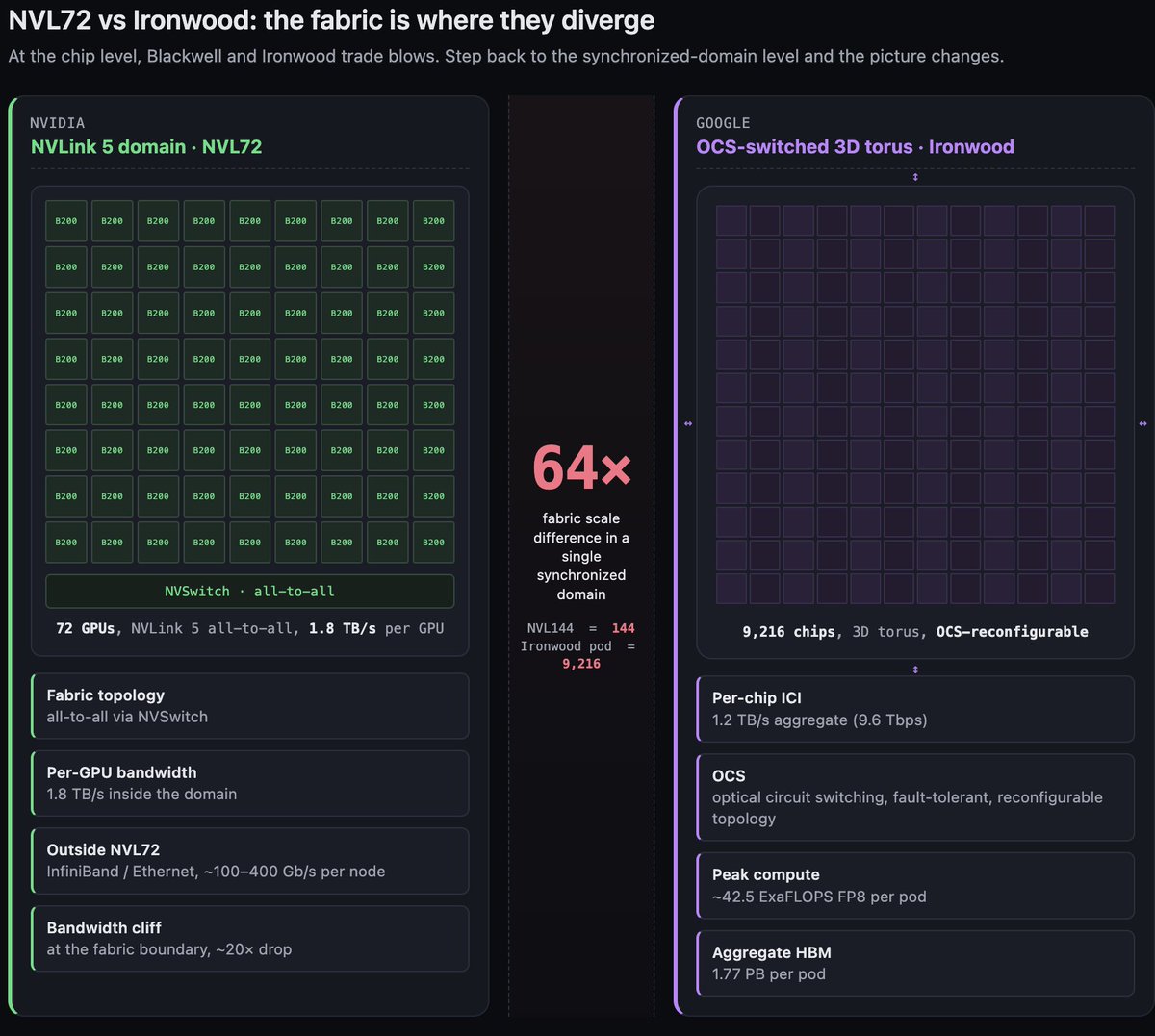
明确的是:NVLink 5 每 GPU 1.8 TB/s,并且 NVL72 成为标准 domain。72 个 GPU 在一个 all-to-all-connected NVLink fabric 中,NVL144 是更大的配置。Blackwell 之前,NVLink domains 在一台服务器里最多到 8 个 GPU。Blackwell 的 NVL72 大了一个数量级。这是对现代训练规模的有意回应,我们会在 §2C 把它和 TPU fabric 故事对比时再谈。
明确的是:通过 NVFP4 进入 FP4 era。NVFP4 是一种两级 scaling format,每 GPU 达到 9 PFLOPS dense,带 sparsity 时 18 PFLOPS;MXFP8 则是八位 microscaling 替代方案。二者都是 Blackwell 上 Transformer Engine 的目标。FP8 峰值数字是每 GPU 4.5 PFLOPS dense,已经接近 Ironwood 的 FP8,使两颗芯片在这个 per-chip 指标上大致可比。
指示性信息,来自 Blackwell microbenchmarking papers 和 vendor tutorials,而不是 NVIDIA 一手文档:Blackwell 引入了 Tensor Memory(TMEM),据报道每 SM 256 KB,这是一个专门用于 Tensor Core operands 的新 near-math storage level。TMEM 位于 SMEM 和 Tensor Core registers 之间。重点是:在 Blackwell 的 Tensor Core throughput 下,就连 SMEM 都离数学太远了,operands 需要活在更近的一层。
指示性信息:tcgen05 是 Blackwell Tensor Core instruction family,公开教程中的描述说 tcgen05 与 warp scheduler 解耦。Tensor Core 有自己的 issue path 和 operand staging。这是 Hopper 趋势的另一半。Hopper 把内存移动从线程中解耦出来,也就是 TMA。Blackwell 把算术从线程中解耦出来,也就是 tcgen05。warp 不再参与 dense linear algebra 的循环。
指示性信息:用于 weight-compressed formats 的 hardware decompression engines,使推理 kernel 可以从 HBM 分页读取加密或压缩权重,并即时解压,而不需要 software pass。
眯着眼看 Blackwell,你会看到一种架构:SM 越来越像 dispatcher,真正的工作发生在那些不再像 Hopper Tensor Cores 那样住在 SM 内部的硬件块里。编程模型通过让作者描述协作来容纳这一点,而底下的机器越来越不可见。表面上仍是 SIMT。底下几乎不再是 SIMT。
GPU 这条线
三代,用三句话说。Ampere 拓宽了高速路。 更高的 Tensor Core peak,更多 HBM bandwidth,async copies,sparsity。Hopper 让移动显式化。 TMA、mbarrier、warpgroups、distributed shared memory。kernel 从循环变成流水线。Blackwell 让 fabric 成为机器。 NVL72、decoupled Tensor Cores、TMEM、microscaling formats。单个 GPU 没有以前那么重要;72-GPU domain 比以前更重要。
把这条线合成一个轨迹:NVIDIA 过去两代一直在沿 SIMT 阶梯向上爬,试图抵达一个位置,在那里由编译器,而不是程序员,来调度数据移动和数学。TMA 是大步。tcgen05 decoupling 是下一步。这是 GPU 栈自己走向 TPU 从一开始就通过构造拥有的东西。
这是一个挑衅性的框架,我是认真这么说的。先把它放在这里,等你继续读下一部分。然后我们会看到 TPU 侧一直站在哪里。
Google 这条线
说明:这些内容都是我加入 Google 前写的,基于我准备期间关于 TPU 的笔记。所有开放数据都来自当时的新鲜笔记,然后我把它写成了人们真的能读懂的形式,而不是我的碎碎念。
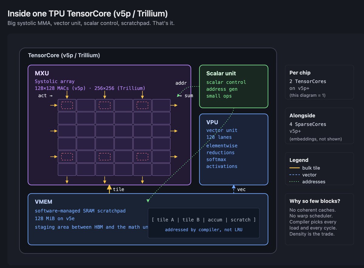
TPU 基础入门
TPU 芯片是一小组大块,而不是许多小块组成的网格。在进入各代之前,把这句话再读一遍。它是最重要的心智模型切换。
一颗 v5p 芯片有两个 TensorCores。一颗 Ironwood 芯片也有两个。Trillium 芯片在 dual-chiplet package 上也有两个。数量少是有意的。每个 TensorCore 都是一台围绕一个主导单元构建的大机器,这个主导单元就是 MXU,旁边围着 vector unit、scalar unit 和 local memory。
MXU 是一个 systolic array。在 v4 和 v5e 上,它是 128×128。在 v5p 上,每芯片仍是 128×128,但芯片里有更多这样的阵列,每个 TensorCore 有两个 MXU。在 Trillium 上,它跳到了 256×256。MXU 做的是密集矩阵数学。它的 dataflow 是 weight-stationary 的一种变体,意思是 weights 停在原地,activations 从中流过。一旦加载了 weights,你就让 activations 穿过网格,累加结果从另一侧流出。tile 适配网格时,吞吐极其夸张。代价是,一切都必须被塑造成适合 MXU 的形状,否则 MXU 就做不了有用的事。
vector unit(VPU)接住 MXU 做不了的一切。Elementwise operations、reductions、softmax interior、layer norm math、activation functions。它是 SIMD-style unit,有自己的 register file 和自己的 lane count。每个 TPU kernel 故事最终都会经过 MXU 和 VPU 的互动:MXU 做 matmul,VPU 做 nonlinearity,编译器用显式数据移动把两者缝起来。
scalar unit 处理控制流、地址生成,以及少数无法表达为 vector 或 matrix units 的操作。它很小。TPU 架构的重点是,把大部分硅面积给 MXU。
TPU 上的内存不像 GPU 内存。这里 没有硬件管理的 L1 或 L2 cache。相反,每颗芯片有 VMEM(Vector Memory),这是一块大的软件管理 SRAM scratchpad。在 v5e 上,每芯片 VMEM 是 128 MiB。后续几代会继续扩展。编译器负责把数据从 HBM 暂存到 VMEM,再从 VMEM 放进 MXU 和 VPU register files。这个细节不能留到后面再藏起来;它是这个平台的定义性特征。
最尖锐的后果,是任何 miss VMEM 的东西都会受到算术强度约束。在 v5e 上,来自 HBM 的 ridge point 大约是每字节 240 FLOPs,而来自 VMEM 的 ridge point 低得多,大概低一个数量级。这意味着,如果你能让一个 tile 常驻 VMEM 并复用它,就只需要低得多的算术强度,也能保持 compute-bound。如果每个操作都必须从 HBM 重新加载,你就需要高得多。TPU 上的每个优化故事,都以这样或那样的方式,讲的是如何让数据尽可能长时间常驻 VMEM。
batch size 是新用户最先被咬到的地方。在 v5e 上,BF16 下每个 replica 需要大约 240 个 token 的 batch,才能超过 HBM ridge point。使用 int8 activations 和 bf16 weights 时,会降到大约 120。低于这些阈值,MXU 会在 HBM 重新填充时闲着。GPU 会随着 batch size 缩小而平滑退化。TPU 会掉下悬崖。修复方式不是更用力地调 kernel,而是重新设计 parallelism strategy,让 per-replica batch 足够大,或者使用更小精度。
ICI(Inter-Chip Interconnect)是 TPU 对应 NVLink 的东西,但更扁平,也更密。在 v5p 上,每芯片 ICI 是 4.8 Tbps,芯片以 3D torus 连接。一个完整 pod 是 8,960 颗芯片。在 Ironwood 上,每芯片 ICI 是 9.6 Tbps,一个 pod 是 9,216 颗芯片。ICI 的重要之处在于,它是 torus,不是 fat tree。每颗芯片都有本地邻居。能很好映射到 torus 的 collective operations,比如 all-reduce、ring-based all-gather,会飞快。需要 global any-to-any 的操作,要么用 Optical Circuit Switching 动态重塑 torus,要么就要付出代价。
SparseCore 是 v4 之后位于 TensorCores 旁边的独立执行单元。它为 MXU 极不擅长的操作设计:sparse embeddings、gather-scatter、hash-table-heavy workloads。v5p 每芯片有四个 SparseCores。每个 SparseCore 有自己的 vector 和 scalar subcores,以及 shared vector SRAM。推荐系统活在 SparseCore 上。LM 中的大词表 embeddings 也一样。
这些够了。下面每一代 TPU 都是这个结构的变体。数 MXU。数 TensorCores。量 VMEM。量 HBM。量 ICI。注意 MXU 是变大、变小,还是保持不变。
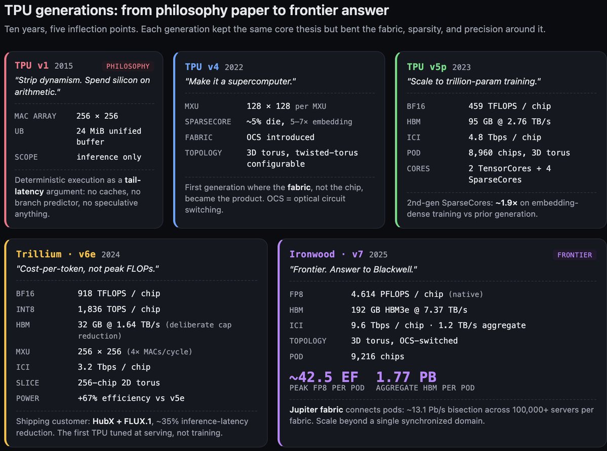
TPU v1:哲学论文
我不想把 v1 写成产品巡礼。它是一颗 2015 年出货的 inference-only chip,有一个 256×256 MAC array,24 MiB 的片上内存,叫 Unified Buffer,还有确定性执行模型。规格不是重点。
重点是 Google 团队在 2017 年写的那篇论文,题为 "In-Datacenter Performance Analysis of a Tensor Processing Unit." 在我看来,它是过去十年里最有后果的架构论文,没有之一,而原因并不是这颗芯片的性能。原因是这篇论文提出了一个激进立场:caches 是坏的,out-of-order execution 是坏的,SMT 是坏的,speculation 是坏的,branch prediction 是坏的,hardware prefetching 是坏的,一切 latency-hiding dynamism 都是坏的。 这些全是为了让不可预测代码看起来很快而花掉的硅面积。ML 工作负载并不可预测。你花在动态性上的每一字节硅,都是没有花在算术单元上的一字节硅。
这就是论点。它至今仍是这条谱系的北极星,我完全同意。如果你想知道 2026 年的 TPU 为什么长这样,就从 2017 年那篇论文开始。
确定性执行部分,是 tail-latency 论点。如果每个操作都提前调度,硬件没有动态性,那么同一程序每次运行都会花同样数量的 cycles。这对训练来说无关紧要,训练看吞吐,不看 tail latency;但对 inference serving 极其重要。确定性加速器不会因为一次调度抖动产生 p99 latency spike。
v1 是推理芯片,它的确定性故事面向推理。v4 之后,同一个论点也开始适用于训练。
v4 和 v5p:通往 Ironwood 的路
我会把 v4 和 v5p 合并成一条线,因为它们讲的是同一个故事,第二次更大而已。先承认 v2 和 v3,这样你不会疑惑:v2 带来了 BF16 和双 TensorCore layout,后续每颗芯片都保留了它。v3 扩大了 MXU array,并加入液冷。二者都不是锚点。v4 才是事情再次变有趣的地方。
v4 引入了两个重塑 TPU pod 的功能。第一个是 SparseCore。v4 大约 5% 的 die area 给了一个独立引擎,用来做 gather-scatter 和 embedding operations,速度是 MXU 无法企及的。在 embedding-heavy workloads 上,SparseCore 相比在 MXU 上跑同样工作能带来 5–7× speedups。它是第一个不是纯 matmul accelerator 的 TPU 功能。
第二个,也是结构上更大的,是 Optical Circuit Switching(OCS)。OCS 允许 Google 在 provisioning time 重新配置 pod 的 interconnect topology。物理 fabric 是由光交换机组成的 3D torus,这些交换机可以重新编程,把不同芯片连接到不同邻居。这带来两个后果。第一,它让 pods 可以针对 workload-specific topologies 重新配置,所以一个受益于 2D slice 的 job 可以拿到一个,而不必布一套独立 fabric。第二,它让 fabric 具备容错性:如果一颗芯片失败,OCS 可以绕开它,pod 以少一颗芯片的状态继续运行。对一个需要同步 8,000+ 颗芯片的 fabric 来说,这种韧性不是锦上添花,而是要求。
v4 还引入了 twisted torus topologies,也就是一些小的拓扑技巧,用来降低 all-to-all collectives 的最坏情况延迟。标准 torus 的最坏 hop count 与边长成正比。twisted torus 把它砍半。这种细节对真实世界的 MFU 很重要,但对没在大规模跑过 collectives 的人完全不重要。
v5p 是放大版 v4。仍然是 3D torus。仍然启用 SparseCore。pod 从 v4 的 4,096 颗芯片增长到 8,960。每颗芯片有 2 个 TensorCores、4 个 SparseCores、95 GB HBM,每芯片带宽 2.76 TB/s,以及每芯片 4.8 Tbps ICI。MXU 每芯片仍是 128×128,但数量更多,所以每芯片 BF16 峰值是 459 TFLOPS。
SparseCore 的收益值得引用:Google 对 v5p 的官方表述是,第二代 SparseCores 让 embedding-dense model training 加速约 1.9×。这是广义的 embedding-heavy workloads,不是专指 MoE。如果你在训练 recommender,或者带非常大词表的 LM,不管你有没有特意要求,SparseCore 都在为你做非平凡的工作。
v5p 是 Google 内部让 trillion-parameter training 变成常规操作的一代。如果你读到过 Gemini 以 petaflop 规模训练,v5p 就是干这活的硬件。
Trillium / v6e:经济性的一代
Trillium 是 TPU 故事变成客户获取故事的地方。核心判断是,Trillium 优化的是每 token 成本,而不是峰值 FLOPs,并且这正在转化为采用率。
规格表本身有趣,但不戏剧性。每芯片 918 TFLOPS BF16、1,836 TOPS INT8、32 GB HBM,每芯片带宽 1.64 TB/s、每芯片 3.2 Tbps ICI、256-chip 2D torus slices。MXU 扩展到 256×256,这让每个 array 每 cycle 的 MAC count 变成四倍。
围绕这些数字的设计决策,才是故事所在。
第一,MXU 跳到 256×256。这让每 cycle MAC count 增加 4×,也把相对于 v5e 的每芯片峰值推高了大致同样倍数。代价是 padding tax。如果你的 matmul tiles 不能在两个轴上都被 256 整除,就会浪费 cycles。Trillium 上的 kernel 作者比在 v5p 上更认真地思考 tile shapes。编译器会做很多 padding,但税是真实存在的。
第二,HBM 容量下降。Trillium 每芯片 32 GB,而 v5p 有 95 GB。这不是倒退,而是有意选择。Trillium 的 pod topology,也就是带强 ICI 的 256-chip 2D torus slices,旨在吸收你原本需要用本地容量支付的 tensor-parallel 和 model-parallel sharding。不是把大 weight shards 保存在每颗芯片上,而是跨更多芯片 sharding,并用 ICI 服务这些 shards。它是 fabric-first memory hierarchy,不是 capacity-first。
第三,功耗故事。Trillium 的 TDP 不是我会引用的公开数字,但已发布的 相比 v5e 能效提升 67% 是干净的 Google 数据。效率是 Trillium 押注的轴线,也是对推理部署最重要的轴线,因为每一瓦都会直接打到你的 per-token cost 上。
Ironwood / v7:锚点世代
Ironwood 是 TPU 侧对 Blackwell 的回答。标题很熟悉。每芯片 4.614 PFLOPS FP8、192 GB HBM3e,每芯片带宽 7.37 TB/s、每芯片 9.6 Tbps ICI,也就是 1.2 TB/s aggregate。按单芯片看,Ironwood 和 B200 在 peak FP8 上处在同一个邻域。这是无聊的部分。
有趣的是 fabric。Ironwood 的 pod 是 9,216 颗芯片组成的 3D torus,通过 OCS 连接。pod-level peak 大约是 42.5 ExaFLOPS。pod-level aggregate HBM 是 1.77 PB。pod 里的每颗芯片都是同一个同步 fabric 的一部分,ICI latency 以数百纳秒计,而不是微秒。
和 Blackwell 对比。NVLink 5 每 GPU 1.8 TB/s。NVL72 是 72 个 GPU,NVL144 是 144 个,二者都在 all-to-all domains 中。超过 NVL144 后,规模必须经过 InfiniBand 或 Ethernet,这会让你从 1.8 TB/s 降到几百 gigabits,latency 也上升超过一个数量级。
Ironwood 的 9,216 是 NVL144 的 64×。这不是一个小数字。在 64× fabric scale 下,每个 parallelism decision 都会改变。在 ICI 成为瓶颈之前,tensor-parallel groups 可以更大。需要 all-to-all communication 的 sharding strategies,在 GPU cluster 上致命的规模,在这里会变得可行。pipeline parallelism 原本是为了掩盖 inter-node latency 而存在的,但由于“inter-node” penalty 小得多,它变得没那么必要。
pod 之外,Google 的 Jupiter fabric 是连接 pods 的数据中心级网络。Jupiter 在每个 fabric 内跨 100,000+ servers 承载大约 13.1 Pb/s 的 bisection bandwidth,Google 在全球运行着数百个这样的 fabrics。它不是某些二手来源偶尔暗示的单一多数据中心网络。它是一个 per-fabric bisection number,适用于一个数据中心部署内部。但这样的部署有很多,总量非常巨大。
Ironwood 也支持类似 MXFP8 的 microscaling precision formats,从而补上 Blackwell 低精度故事的差距。更大的架构变化是,Ironwood 的 TensorCore 在 tile 如何被喂入、MXU 如何与 VPU 组合、编译器如何调度 bundles 来保持 pipeline 满载方面更灵活。我不会展开每个微优化。标题是:FP8 是原生的,HBM3e 匹配或超过 Blackwell 的每芯片带宽,而 fabric 是主导性差异。
如果你从这里带走一件事,就带走 fabric comparison。9,216 对 144。单个同步 domain 内 64×。其他每个规格都在两家厂商之间收敛。fabric 没有。
TPU 这条线
五代,用五句话。v1 证明了这个论点:ML accelerators 应该剥掉动态性,把硅面积花在算术单元上。v4 把它变成了超级计算机,通过 SparseCore 和 OCS。v5p 扩展到 trillion-parameter training,并且架构没有断。Trillium 让它便宜,通过押注经济性而不是 headline FLOPs。Ironwood 让它进入前沿,通过赶上 FP8,并把 fabric advantage 扩展到 NVLink-domain scale 的 64×。
把这条线合成一个轨迹:TPU 谱系一直在下注,认为 compiler-scheduled determinism、systolic matrix density 和 fabric-first scale,比 SIMT flexibility、cache hierarchies 和 per-node optimization 更能产生复利。在前沿规模上,这个下注正在兑现。Article 2 会解释为什么这个下注在 kernel-author scale 上也会兑现,而按传统看法,那里本该是 GPU 赢的地方。
import triton
import triton.language as tl

@triton.jit
def matmul_kernel(
    a_ptr, b_ptr, c_ptr,
    M, N, K,
    stride_am, stride_ak,
    stride_bk, stride_bn,
    stride_cm, stride_cn,
    BLOCK_M: tl.constexpr,
    BLOCK_N: tl.constexpr,
    BLOCK_K: tl.constexpr,
):
    pid_m = tl.program_id(0)
    pid_n = tl.program_id(1)

    offs_m = pid_m * BLOCK_M + tl.arange(0, BLOCK_M)
    offs_n = pid_n * BLOCK_N + tl.arange(0, BLOCK_N)
    offs_k = tl.arange(0, BLOCK_K)

    a_ptrs = a_ptr + offs_m[:, None] * stride_am + offs_k[None, :] * stride_ak
    b_ptrs = b_ptr + offs_k[:, None] * stride_bk + offs_n[None, :] * stride_bn

    acc = tl.zeros((BLOCK_M, BLOCK_N), dtype=tl.float32)
    for k in range(0, K, BLOCK_K):
        a = tl.load(a_ptrs)
        b = tl.load(b_ptrs)
        acc += tl.dot(a, b)
        a_ptrs += BLOCK_K * stride_ak
        b_ptrs += BLOCK_K * stride_bk

    c_ptrs = c_ptr + offs_m[:, None] * stride_cm + offs_n[None, :] * stride_cn
    tl.store(c_ptrs, acc.to(tl.float16))
两条线在哪里相撞
我们已经走完两边。现在,我来点出那些地方。在那里,两条线看起来不再像平行故事,而更像是对同一个问题给出的不同答案。
内存层级分歧,通过增加发生。 GPU memory hierarchies 每一代都在 增加 near-math tiers。早期 Volta 上的 SMEM。Ampere 上 L1-combined SMEM。Hopper 上的 Distributed Shared Memory。Blackwell 上的 Tensor Memory。每一层都比前一层更靠近数学。TPU 从一开始就有 VMEM。TPU 不需要增加新的 near-math tier;它本来就是围绕这个东西设计的。GPU 架构师一直在构建的,是 SIMT 模型内部逐层形成的某种 VMEM。
移动分歧,通过承认发生。 Hopper 上的 TMA,是 NVIDIA 承认 descriptor-driven async transfers 才是在 Tensor Core throughput 下移动数据的方式。TPU 上的数据一直就是这样移动的,因为做调度的是编译器,不是线程。Hopper descriptor model,包括 source tensor shape、destination SMEM layout、swizzle、OOB fill、mbarrier gate,是 Mosaic 一直为 MXU 生成的那类调度的后代。
执行模型分歧,通过解耦发生。 Blackwell 的 tcgen05 把 Tensor Cores 从 warp scheduler 中解耦出来。warp 不再参与 dense arithmetic 的循环。这是一次结构性变化,让矩阵引擎更像一个有自己 issue path 的协作块。在 TPU 上,MXU 从一开始就没有 warp scheduler。编译器给阵列喂一个 tile,阵列节奏完成数学,结果落到编译器指定的位置。NVIDIA 正在逐步让 Tensor Cores 更像 systolic pipeline,同时仍在向程序员呈现线程模型。
规模分歧,通过 fabric 发生。 NVL72 是 72 个 GPU,NVL144 是 144 个。Ironwood 是单个 OCS-switched torus 中的 9,216 颗芯片。这是同步 domain 内的 64×。前沿规模上的每个 parallelism decision 都取决于这个比例。这是两条线尚未收敛的一条轴,也是设计哲学分歧最清楚的一条轴。NVIDIA 的 fabric 从 8 增长到 144,之后是 InfiniBand。Google 的 fabric 从数百增长到数千,仍在一个同步 OCS torus 中,之后是 Jupiter。
精度收敛,通过多条路径发生。 两套栈都在落向 FP8,把它作为标准训练精度,下一步是 microscaling formats,比如 NVFP4、MXFP8。Blackwell 通过从 Hopper 的 Transformer Engine 迭代到达那里。Ironwood 通过直接跳到原生 FP8,到达那里并追上。路径不同,目的地相同。
现在到了前沿规模的重点。这件事我从一开始就在铺垫。
PaLM 540B 在 6,144 颗 TPU v4 芯片 上训练,达到 46.2% model FLOPs utilization。PaLM 论文把它描述为“pipeline-free training”。他们在 3D torus 上运行纯 data 加 model,也就是 tensor parallelism。两个 v4 pods,通过 DCN 连接。完全没有 pipeline parallelism。v4 fabric 的形状让他们能跳过 pipeline。
Llama 3 405B 在 16,384 个 H100 上训练,MFU 大约是 38–43%。Llama 3 论文描述了 4D parallelism:tensor,一个 matmul 跨芯片 sharding;pipeline,不同 layer 放在不同芯片上,activations 按 stage 向前传;context,长序列跨芯片切分;data,同一模型跑不同 batch,并用 FSDP sharding parameters。四个轴,因为 NVLink domain 本身装不下完整 tensor-parallel group,而 NVLink 之外的 InfiniBand fabric 又无法在所需规模上吸收 all-to-all,于是 pipeline parallelism 不得不掩盖这两个缺口。
两个 MFU 处在接近范围。一个用了两个 parallelism 轴达到。另一个用了四个。原因是 bandwidth hierarchy 的形状。PaLM 的 v4 fabric 足够平,data 和 tensor parallelism 就能吸收计算。Llama 3 的 H100 fabric 在 NVLink 和 InfiniBand 之间有一道悬崖,而填平这道悬崖需要 pipeline 和 context parallelism 作为补救。
每个 cluster 的 bandwidth hierarchy 形状,会决定你被允许选择什么 parallelism strategy。这就是前沿规模上的事实。
记住它。Article 2 明天发布,讲的是同样的 shape-constrains-strategy 逻辑是否也会在 kernel scale 上发生,而不只是在 cluster scale 上。我的判断是会。我们会在 Article 2 遇到的编程模型,不是这些架构之上的中性选择。它们是架构通过软件开口说话。
收起这个大怪物
这就是架构基础。两种哲学,两边各自大约五代,一堵内存墙塑造全局,一个 fabric gap 分开两个前沿。
带着三件事继续往后读。
-
内存墙是主角。本文里的每个缩写词,都是让数据靠近数学的不同工具。
-
SIMT 和 systolic 不是同一种关于如何喂饱矩阵乘的赌注。NVIDIA 赌的是有生产力的线程,并且过去两代一直在线程下方加入 compiler-scheduled machinery。Google 赌的是 compiler-scheduled systolic core,并在它周围增加灵活性。
-
在前沿规模上,fabric 已经成为差异点。9,216 对 144,是同步 domain 内的 64× 差距,而这个比例会重塑你被允许使用的 parallelism strategy。
Article 2 会从这里接上。我们会用刚才这种平行游览的形状,讲 NVIDIA stack(CUDA、CUTLASS、cuDNN、Triton、frameworks)和 Google stack(XLA、StableHLO、JAX、Pallas、Mosaic、PyTorch/XLA)。然后进入带立场的论证:我会论证,composition、compiler leverage 和 profiler tooling 叠起来,会在 GPU 本该完全占据优势的地方,也就是 custom kernel authoring,形成优势。最后是一份给我这种位置上的工程师看的 Triton-to-Pallas migration playbook。
从 Meta 到 Google 的转变发生得很快,但心智模型的转变慢一些。Article 2 一部分是技术论证,一部分也是这次转变的记录。两者都是。
到那里见。